What Does 3nm or 5nm Mean in Chips?
When you hear about a new smartphone with a "3nm chip" or a laptop powered by "5nm technology," these numbers refer to the manufacturing process used to create the processor. The nanometer measurement describes the size of transistors packed onto the silicon wafer, with smaller numbers indicating more advanced technology.
The Basics of Nanometer Measurements
A nanometer equals one billionth of a meter. In chip manufacturing, this measurement originally represented the physical dimensions of transistors on a processor. Modern 3nm and 5nm chips contain billions of these tiny switches that perform calculations and store data. When manufacturers shrink transistor size, they can fit more processing power into the same physical space.
The relationship between nanometer measurements and actual transistor dimensions has become less direct in recent years. What started as a literal measurement now serves more as a generation marker. A 3nm chip doesn't necessarily have components measuring exactly 3 nanometers, but it represents a manufacturing generation more advanced than 5nm technology.
Performance Benefits of Smaller Processes
Smaller transistors deliver three major advantages. First, they consume less power because electrons travel shorter distances between components. This translates to longer battery life in mobile devices and reduced energy costs in data centers. Second, tighter transistor packing increases processing density, allowing chips to execute more operations simultaneously. Third, reduced size enables faster switching speeds since electrical signals need less time to traverse shorter pathways.
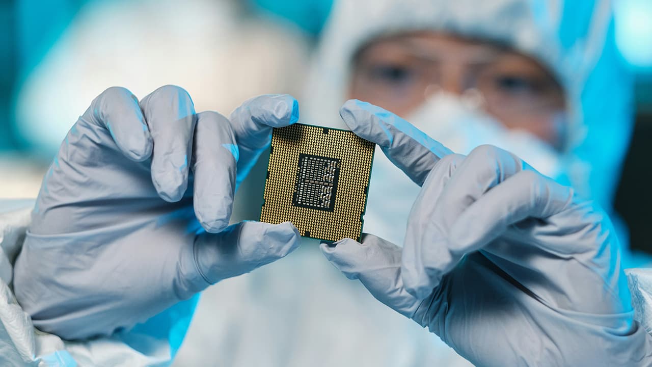
A 3nm processor can contain approximately 300 million transistors per square millimeter, compared to roughly 170 million in 5nm chips. This dramatic increase in density means manufacturers can either create more powerful processors in the same physical footprint or maintain similar performance while reducing chip size and cost.
Manufacturing Challenges
Creating chips at these scales presents enormous technical hurdles. Manufacturers must use extreme ultraviolet lithography, which employs light with wavelengths around 13.5 nanometers to etch circuit patterns onto silicon wafers. The precision required approaches the atomic level, where even minor contamination or vibration can ruin entire batches.
Production facilities for advanced nodes cost billions of dollars to build and maintain. Only a handful of companies worldwide possess the expertise and resources to manufacture 3nm and 5nm chips. These foundries operate in ultra-clean environments where air purity exceeds operating room standards by orders of magnitude.
The Future of Chip Manufacturing
Industry roadmaps already outline plans for 2nm and even 1nm processes. Each new generation requires innovative solutions to physics problems that become more pronounced at smaller scales. Quantum effects, heat dissipation, and power leakage all intensify as transistors shrink.
Alternative approaches like chiplet designs and 3D stacking offer ways to increase performance without solely relying on smaller transistors. These methods connect multiple chips or stack them vertically, creating powerful processors that combine different manufacturing processes.
The race toward smaller nanometer measurements continues because performance demands keep growing. Whether for artificial intelligence, scientific computing, or everyday consumer devices, the push for more efficient and powerful chips drives innovation in semiconductor manufacturing.


